
 Product
 Brand
Brand Articles
 Tools
Tools
An Overview of 12 Important CPU Specs
Understanding CPU Specs - CPU Specs Guide for Beginners
Catalog | |
| |
Ⅰ Introduction
CPUs generally consist of a logical computing unit, a control unit, and a storage unit. The logical operation and control units include some registers, which are used for the temporary storage of data during the CPU processing. The CPU specs you see when you buy a CPU on the market are generally in the format of (main frequency/front side bus/secondary cache). For example, the Intel P6670 is (2.16GHz\800MHz\2MB).
Ⅱ Main CPU specifications
CPU specifications include main frequency, multiplier, external frequency, bus frequency, L2 cache, operating voltage, interface and manufacturing process, etc.
The main CPU specs that you need to focus on are as follows.
1. Main Frequency
The main frequency is the clock frequency of the CPU, which simply means the operating frequency of the CPU. For example, we often say P4 (Pentium IV) 1.8GHz, this 1.8GHz (1800MHz) is the CPU's main frequency. Generally speaking, the number of instructions completed in one clock cycle is fixed, so the higher the main frequency, the faster the CPU will be. Main frequency = external frequency X multiplier.
The main frequency of the CPU is not directly related to the actual computing power of the CPU. The main frequency indicates the speed at which digital pulse signals oscillate within the CPU. We can see examples of this in Intel's processor products: 1 GHz Itanium (Anthem) chips can perform almost as fast as 2.66 GHz Xeon/Opteron. The speed of the CPU also depends on the performance of the CPU pipeline in all aspects.
Of course, there is a correlation between the main frequency and the actual computing speed, but it can only be said that the main frequency is only one aspect of the CPU specifications, not the overall performance of the CPU.
2. External Frequency
The external frequency is the external clock frequency of the CPU. The main standard external clock frequencies for motherboards and CPUs are 66MHz, 100MHz, and 133MHz. In addition, the more and higher the adjustable external frequency of the motherboard the better, especially for overclockers is more useful.
By external frequency, we mean the speed at which the CPU is connected to the motherboard, a concept that is based on the oscillating speed of the digital pulse signal.
The CPU's external frequency determines the operating speed of the entire motherboard. In desktop computers, when we talk about overclocking, we are talking about overclocking the CPU's external frequency (of course, in general, the CPU's multiplier is locked). But for server CPUs, overclocking is absolutely not allowed. As mentioned earlier, the CPU determines the operating speed of the motherboard, the two are running synchronously, if the server CPU is overclocked, changing the external frequency, will produce asynchronous operation, (desktop many motherboards support asynchronous operation) which will cause the entire server system instability.
The vast majority of current computer systems are also synchronized between memory and motherboard running speed. In this way, it can be understood that the CPU's external frequency is directly connected to the memory to achieve a synchronous state of operation between the two. It is very easy to confuse external clock with front-side bus (FSB) frequency.
3. Front Side Bus (FSB) Frequency
Front Side Bus (FSB) frequency (i.e. bus frequency) is a direct impact on the speed of direct data exchange between CPU and memory. The front-end bus frequency has two concepts: one is the physical operating frequency of the bus (that is, what we call the external frequency), and the other is the effective operating frequency (that is, what we call the FSB frequency) which directly determines the data transfer speed of the front-end bus!
INTEL processor's relationship between the two is: FSB frequency = external frequency X4; and AMD's is: FSB frequency = external frequency X2.
FSB is usually used to indicate that it is the bus that connects the CPU to the Northbridge chip.
The difference between the external frequency and the front side bus (FSB) frequency: the speed of the front side bus refers to the speed of data transfer, while the external frequency is the speed of synchronous operation between the CPU and the motherboard.
4. CPU bits and word length
Bit: In digital circuits and computer technology, binary is used, the code is only "0" and "1", where either "0" or "1 " in the CPU is a "bit".
Word length: The number of bits of binary numbers that the CPU can process at one time per unit of time (at the same time) is called word length in computer technology. So a CPU that can handle 8 bits of data is usually called an 8-bit CPU, and a 32-bit CPU can handle 32 bits of binary data per unit of time. The difference between byte and word length: Since common English characters can be represented by 8-bit binary, 8 bits are usually called a byte. The length of the word length is not fixed and varies for different CPUs. 8-bit CPUs can only process one byte at a time, while 32-bit CPUs can process 4 bytes at a time, and similarly, a 64-bit CPU can process 8 bytes at a time.

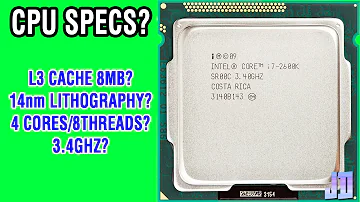
Intel CPU specs comparison
5. Multiplier
Multiplier refers to the number of times the CPU's external frequency differs from the main frequency. For example, the CPU of Athlon XP 2000+ has an external frequency of 133MHz, so its multiplier is 12.5 times.
Initially, the CPU did not have the concept of the multiplier. It had the same speed of main frequency and external frequency, but as the CPU speed became faster and faster, the multiplier technology came into being. Its biggest function is to enable the system bus to work at a relatively low frequency, and the CPU speed is infinitely increased.
6. Interface
Interface refers to the interface between the CPU and the motherboard. There are two main categories, one is the card interface, called SLOT. Card interface CPUs are like the various expansion cards we often use, such as graphics cards, sound cards, etc... They are plugged into the motherboard vertically. Of course, the motherboard must have the corresponding SLOT slot, this interface CPU has been eliminated. Another category is the mainstream pin-type interface, called Socket, Socket interface CPU has hundreds of pins because the number of pins are different and is called Socket370, Socket478, Socket462, Socket423, etc...
7. Cache
A cache is a memory that can exchange data at high speed. It takes precedence over memory to exchange data with the CPU, so it is extremely fast, so it is also called a cache. There are generally two types of caches associated with processors - L1 cache, also known as internal cache, and L2 cache, also known as an external cache. For example, the Pentium 4 "Willamette" core product has a 423-pin architecture, a 400MHz front-end bus, 256KB of full-speed L2 cache, 8KB of Level 1 trace cache, and the SSE2 instruction set.
L1 Cache (Level 1 Cache) is the first level of CPU cache, which is divided into the data cache and instruction cache. The capacity of the L1 cache of general server CPUs is usually 32-256KB.
L2 Cache (Level 2 Cache) is the second level of CPU cache, divided into internal and external chips.
L3 Cache (Level 3 Cache), the application of L3 cache can further reduce memory latency while improving processor performance during large data volume calculations. Reducing memory latency and improving the ability to compute large amounts of data are both helpful for gaming.
Internal cache (L1 Cache)
The internal cache is also often referred to as the first-level cache. The built-in cache inside the CPU can improve the CPU's operation efficiency. The larger the L1 cache is, the less data is exchanged between the CPU and the slower L2 cache and memory, which can increase the computer's computing speed. However, cache memory is composed of static RAM and has a complex structure. In the case of CPU, the core area cannot be too large, the capacity of the L1 level cache can not be too large, and the capacity unit of the L1 cache is generally KB.
External cache (L2 Cache)
CPU external cache. External cache cost is expensive, so the Pentium 4 Willamette core for external cache 256K, but the same core of the Celeron 4 generation only 128K.
8. Instruction set
(1) CISC instruction set
CISC instruction set, also known as complex instruction set (abbreviation of Complex Instruction Set Computer).
(2) RISC instruction set
RISC is the abbreviation of "Reduced Instruction Set Computing".
(3) IA-64
Breakthrough many limitations of the traditional IA32 architecture, in the data processing capacity, system stability, security, availability, viewability and other aspects of a breakthrough improvement.
(4) X86-64 (AMD64 / EM64T)
IA-64 breaks through many of the limitations of the traditional IA32 architecture and achieves breakthrough improvements in data processing power, system stability, security, availability, and viewability.
Multimedia instruction set
In order to improve the ability of computers in multimedia and 3D graphics applications, many processor instruction sets have been created, and the three most famous ones are Intel's MMX, SSE/SSE2, and AMD's 3D NOW! Theoretically, these instructions play a comprehensive role in enhancing popular image processing, floating-point computing, 3D computing, video processing, audio processing, and many other multimedia applications.
9. Manufacturing Process
Early processors were manufactured using a 0.5-micron process. As CPU frequencies increased, the original process could no longer meet the requirements of the product, so the 0.35 micron and 0.25-micron processes emerged. The finer the process means more electronic components are integrated per unit volume. 0.18-micron and 0.13-micron processor products are the mainstream in the market, for example, Northwood core P4 uses a 0.13-micron production process. In 2003, Intel and AMD's CPU manufacturing process will reach 0.09 micron.
10. Voltage
CPU operating voltage (Vcore) refers to the voltage required for normal CPU operation and is related to the production process and the number of integrated transistors. The lower the voltage for normal operation, the lower the power consumption and the less heat generation. The direction of CPU development is to keep reducing the voltage required for normal operation on the basis of guaranteed performance. For example, the operating voltage of the old core Athlon XP is 1.75v, while the voltage of the new core Athlon XP is 1.65v.
11. Package Form
CPU package is the last process in the CPU production process. The package is a protective measure to prevent damage to the CPU chip or CPU module by curing it with a specific material. The CPU packaging method depends on the form of CPU mounting and device integration design. In general, CPUs mounted in socket sockets are usually packaged in PGAs (grid arrays), while CPUs mounted in Slot x slots are all packaged in SECs (single-sided connector boxes). There are also package technologies such as PLGA (Plastic Land Grid Array) and OLGA (Organic Land Grid Array). Due to the increasing competition in the market, the development direction of the former CPU package technology is based on cost-saving.
12. Unit
ALU - Arithmetic Logic Unit, which is what we call "integer" unit. Mathematical operations such as addition, subtraction, multiplication, and division and logical operations such as "OR, AND, ASL, ROL" are executed in the ALU. In most software programs, these operations make up the majority of the program code.
The floating-point unit (FPU) is mainly responsible for floating-point operations and high precision integer operations. Some FPUs also have the function of vector operations, and some others have dedicated vector processing units.
The integer processing capability is the most important manifestation of CPU computing speed, but the floating-point operation capability is an important indicator related to the CPU's multimedia and 3D graphics processing, so for modern CPUs, the strength of the floating-point unit computing capability is more indicative of the CPU specification.
 UTMEL
UTMEL
We are the professional distributor of electronic components, providing a large variety of products to save you a lot of time, effort, and cost with our efficient self-customized service. careful order preparation fast delivery service
1. What is the most important CPU spec?
Cores. The core count is the spec most commonly flaunted by CPU manufacturers today, so what are cores, what purpose do higher core counts serve, and is a high core count important for gaming? To put it simply, a core is a processor. In the past, CPUs had only one core.
2. What is CPU specification mean?
The clock speed (commonly referred to as the frequency) of a CPU is how many instructions per second it can process and is typically reported in MHz or GHz. For example, a 3GHz (or 3000MHz) processor can complete 3,000,000,000 instructions per second.
 Discovering New and Advanced Methodology for Determining the Dynamic Characterization of Wide Bandgap DevicesSaumitra Jagdale15 March 20242674
For a long era, silicon has stood out as the primary material for fabricating electronic devices due to its affordability, moderate efficiency, and performance capabilities. Despite its widespread use, silicon faces several limitations that render it unsuitable for applications involving high power and elevated temperatures. As technological advancements continue and the industry demands enhanced efficiency from devices, these limitations become increasingly vivid. In the quest for electronic devices that are more potent, efficient, and compact, wide bandgap materials are emerging as a dominant player. Their superiority over silicon in crucial aspects such as efficiency, higher junction temperatures, power density, thinner drift regions, and faster switching speeds positions them as the preferred materials for the future of power electronics.
Read More A Comprehensive Guide to FPGA Development BoardsUTMEL11 September 202520578
This comprehensive guide will take you on a journey through the fascinating world of FPGA development boards. We’ll explore what they are, how they differ from microcontrollers, and most importantly, how to choose the perfect board for your needs. Whether you’re a seasoned engineer or a curious hobbyist, prepare to unlock new possibilities in hardware design and accelerate your projects. We’ll cover everything from budget-friendly options to specialized boards for image processing, delve into popular learning paths, and even provide insights into essential software like Vivado. By the end of this article, you’ll have a clear roadmap to navigate the FPGA landscape and make informed decisions for your next groundbreaking endeavor.
Read More 800G Optical Transceivers: The Guide for AI Data CentersUTMEL24 December 202510974
The complete guide to 800G Optical Transceiver standards (QSFP-DD vs. OSFP). Overcome supply shortages and scale your AI data center with Utmel Electronic.
Read More The 2026 Engineer’s Guide: Choosing the Right MCU for Your Next IoT & New Energy ProjectUTMEL30 April 2026908
A comprehensive comparison of 2026's leading MCUs from ST, NXP, and Microchip across power efficiency, processing performance, connectivity, and ecosystems to help engineers select the optimal chip for next-gen IoT and new energy projects.
Read More AI Server Components: Engineering Next-Gen Data Center Hardware for 100kW RacksUTMEL15 May 2026432
The transition from traditional enterprise IT to AI-driven workloads has rendered legacy data center hardware obsolete, forcing infrastructure planners to re-engineer server components for extreme thermal environments.
Read More
Subscribe to Utmel !
![MOC3010SM]() MOC3010SM
MOC3010SMON Semiconductor
![ADATE320-1KCPZ]() ADATE320-1KCPZ
ADATE320-1KCPZAnalog Devices Inc.
![AT88SC0104CA-SU]() AT88SC0104CA-SU
AT88SC0104CA-SUMicrochip Technology
![MOC3162M]() MOC3162M
MOC3162MON Semiconductor
![80HCPS1848CBLGI]() 80HCPS1848CBLGI
80HCPS1848CBLGIRenesas Electronics America Inc.
![HCS500-I/P]() HCS500-I/P
HCS500-I/PMicrochip Technology
![AD8190ACPZ-R7]() AD8190ACPZ-R7
AD8190ACPZ-R7Analog Devices Inc.
![ATA663231-GBQW]() ATA663231-GBQW
ATA663231-GBQWMicrochip Technology
![AD9942BBCZ]() AD9942BBCZ
AD9942BBCZAnalog Devices Inc.
![ATAES132A-SHEQ-B]() ATAES132A-SHEQ-B
ATAES132A-SHEQ-BMicrochip Technology


